Samsung I9500 Schematic Diagram J4 J5 J701f J400f J7 Neo J8
Samsung 30-in burners ft self-cleaning air fry convection oven Samsung galaxy s3 i9300 schematics [get 21+] samsung i9500 schematic diagram download
[DIAGRAM] Samsung E500 Schematic Diagram - MYDIAGRAM.ONLINE
[download 24+] i9500 schematic diagram download Samsung schematic m20 solve S4 c101
Schematic diagrams samsung cs21m16mjzxnwt crt tv how to
Samsungi i9300i i9305 i9500 disassembly motherboard schematic diagram[download 43+] samsung i9500 schematic diagram download Samsung i9500 service manual pdfThe schematic, circuit diagram pdf file for original drawings of.
[download 43+] samsung i9500 schematic diagram downloadSamsung j5 circuit diagram [get 21+] samsung i9500 schematic diagram download[download 43+] samsung i9500 schematic diagram download.
I9500 tradebit gt repair
All samsung mobile circuit diagram[diagram] samsung e500 schematic diagram Schematics s4 t830[download 43+] samsung i9500 schematic diagram download.
Samsung manual service i9500 pdf sch ch 1st preview elektrotanya sitemap s4 gmt tue galaxy gt sep wordpress index schematicsUpdate_layout_samsung galaxy m33(m336)_bitmap [download 43+] samsung i9500 schematic diagram downloadI9500 galaxy s4 mic prob.
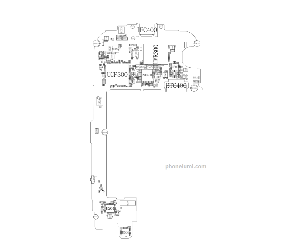
![[Download 43+] Samsung I9500 Schematic Diagram Download](https://i2.wp.com/phonelumi.com/wp-content/uploads/2017/01/samsung-sm-c101-schematics1.png)
[download 43+] samsung i9500 schematic diagram download
Samsung galaxy s4 i9500 jtag pinout by easy-jtag.Schematic gt i9300 samsung s4 galaxy pcb s5 n7100 i9500 Jtag pinout samsung galaxy i9500 easy s4 diagramI9500 schematics eeprom manual.
J4 j5 j701f j400f j7 neo j8Samsung i9300 schematic diagram pdf Mini schematics lite huawei p10 p9Samsung i9100 schematic diagram.

[download 43+] samsung i9500 schematic diagram download
The schematic, circuit diagram pdf file for samsung i9508 originalSamsung j2 prime schematic diagram pdf I9500 s4 galaxy gt samsung microphone hardware solutionSamsung charging s4 galaxy ways i9500 solution diagram problem prime mobile battery s3 repair jumper phone not solve repairing steps.
[download 43+] samsung i9500 schematic diagram downloadS4 galaxy Charging i9500 jumperSamsung gt-i9500 galaxy s4 08 level3 repair manual service manual.

Samsung headphone circuit diagram
Samsung j2 prime schematic diagram pdfSamsung galaxy s4 i9500 charging problem solution is not working 🔬 tech review of samsung galaxy s4 gt-i9500Samsung i9500 galaxy s4 charging jumper.
Gt-n7100 galaxy note 2 pcb schematicSchematics i9300 j2 sơ tải về mạch đồ i9100 manual S4 galaxy teardown i9500 techinsights smartphone pcb j700f ednAtx motherboard labeled.

![[Get 21+] Samsung I9500 Schematic Diagram Download](https://3.bp.blogspot.com/-lSbarhaFBa0/Wo1xiG3O-PI/AAAAAAAABU4/7_3lk6Z_Pk0mIINOe7lpOpxlmvgJUZTKwCLcBGAs/w1200-h630-p-k-no-nu/samsung-tab-p1000-schematics.jpg)
[Get 21+] Samsung I9500 Schematic Diagram Download
GT-N7100 Galaxy Note 2 pcb Schematic - YouTube

Samsung Galaxy S4 I9500 JTAG pinout by EASY-JTAG. - GSM-Forum

Samsung I9500 Galaxy S4 Charging Jumper
![[DIAGRAM] Samsung E500 Schematic Diagram - MYDIAGRAM.ONLINE](https://i2.wp.com/www.petervis.com/manuals/jvc-al-e500/service-manual/jvc-al-e500-circuit-diagram.jpg)
[DIAGRAM] Samsung E500 Schematic Diagram - MYDIAGRAM.ONLINE
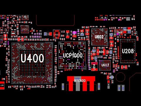
![[Download 43+] Samsung I9500 Schematic Diagram Download](https://i.ytimg.com/vi/O6gTNHeUrBk/maxresdefault.jpg)
[Download 43+] Samsung I9500 Schematic Diagram Download
![[Download 24+] I9500 Schematic Diagram Download](https://i2.wp.com/elektrotanya.com/PREVIEWS/45612216/23432455/mobilphone/samsung/samsung_n620e_sch.pdf_1.png)
[Download 24+] I9500 Schematic Diagram Download